Examples of nanoindentation data
Please look at the experimental procedure proposed by Jennett N. M. and Bushby A. J. [1], to perform nanoindentation tests on bulk, coatings or multilayer systems, and to the ISO standard (ISO 14577 - 1 to 4).
Type of data - Pre-Requirements
Only data from Continuous Stiffness Measurement (CSM), given as a function of the indentation depth are accepted in the NIMS toolbox (e.g.: CSM mode for Agilent - MTS nanoindenter or DMA - CMX algorithm for Hysitron nanoindenter).
You data must only have the loading part from the load-displacement curves of your (nano)indentation results. In the case of data saved in a ‘Sample’ or ‘Analyst Project’ sheet of a .xls file obtained with ‘Analyst’ (MTS software) (containing at least a ‘Hold Segment Type’ or a ‘END’ segment), the toolbox is able to consider only the loading part of your results.
Please, check if the surface detection is well done, especially if the substrate is compliant [2] and [4]. For more explanations about the surface detection, look into the NIMS documentation.
It is advised to use average results from at least 10 indentation tests to avoid artefacts (e.g. pop-in, roughness, local impurities or dust on the sample’s surface…).
Note
To analyze pop-in distribution, the Matlab PopIn toolbox was developed. The Matlab code is available on GitHub with the documentation.
Agilent - MTS example files
Both .txt or .xls files are accepted.
3 columns (Displacement / Load / Stiffness)
6 columns (Disp. / SD (Disp.) / Load / SD (Load.) / Stiff. / SD (Stiff.)) (SD for Standard Deviation)
It is possible to get directly these type of average sheet in your .xls file, using the ‘Analyst’ Excel macro provided by MTS.
- MTS_0film_Si_CSM-2nm_noSD.txt
Data for a bulk Silicon sample.
Data obtained by Berkovich indentation with CSM mode (75Hz / amplitude 2nm) (no standard deviation).
- MTS_1film_SiO2_Si_CSM-2nm.xls
Data for a thin film of Silicon thermal oxide (500nm) on a bulk Silicon sample.
Data obtained by Berkovich indentation with CSM mode (75Hz / amplitude 2nm).
- MTS_1film_SiO2_Si_CSM-2nm_noSD.xls
Data for a thin film of Silicon thermal oxide (500nm) on a bulk Silicon sample.
Data obtained by Berkovich indentation with CSM mode (75Hz / amplitude 2nm) (no standard deviation).
- MTS_2films_Al_SiO2_Si_CSM-2nm.xls
Data for a thin film of PVD Aluminum (500nm) deposited on a bulk Silicon sample with a Silicon thermal oxide (500nm).
Data obtained by Berkovich indentation with CSM mode (75Hz / amplitude 2nm).
- MTS_3films_Au-Ti-SiO2-Si_CSM-1nm.txt
Data for a thin film of PVD Gold (500nm) deposited on thin film of PVD Titanium (500nm) on a bulk Silicon sample with a Silicon thermal oxide (500nm).
Data obtained by Berkovich indentation with CSM mode (75Hz / amplitude 1nm).
- MTS_3films_Au-Ti-SiO2-Si_CSM-1nm.xls
Data for a thin film of PVD Gold (500nm) deposited on thin film of PVD Titanium (500nm) on a bulk Silicon sample with a Silicon thermal oxide (500nm).
Data obtained by Berkovich indentation with CSM mode (75Hz / amplitude 1nm).
The last example (2 files for Au-Ti-SiO2-Si sample) is used to validate the elastic multilayer model of Mercier et al. [3]. A micrograph of this sample is given Figure 33.
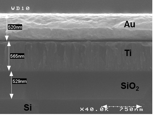
Figure 33 SEM cross-sectional observation of a multilayer sample.
Hysitron example files
Both .txt or .dat files are accepted.
- Hysitron_dma.txt
Data obtained by Berkovich indentation with DMA mode (205Hz / amplitude 0.65nm) - Courtesy of Dr. Igor Zlotnikov from Max Planck Institute of Colloids and Interfaces in Potsdam, Germany.